
Building the future of semiconductor manufacturing.
Let’s engineer the infrastructure behind tomorrow's technology.
Access decades of experience in semiconductor fabrication with a team that has participated in the design and construction of multiple fabrication facilities in Silicon Valley and worked in fabs around the world. Our experience provides a practical understanding of how fabrication facilities operate from the user’s perspective and how to translate that knowledge into effective facility and tool environments.
Hover to explore our expertise.
01
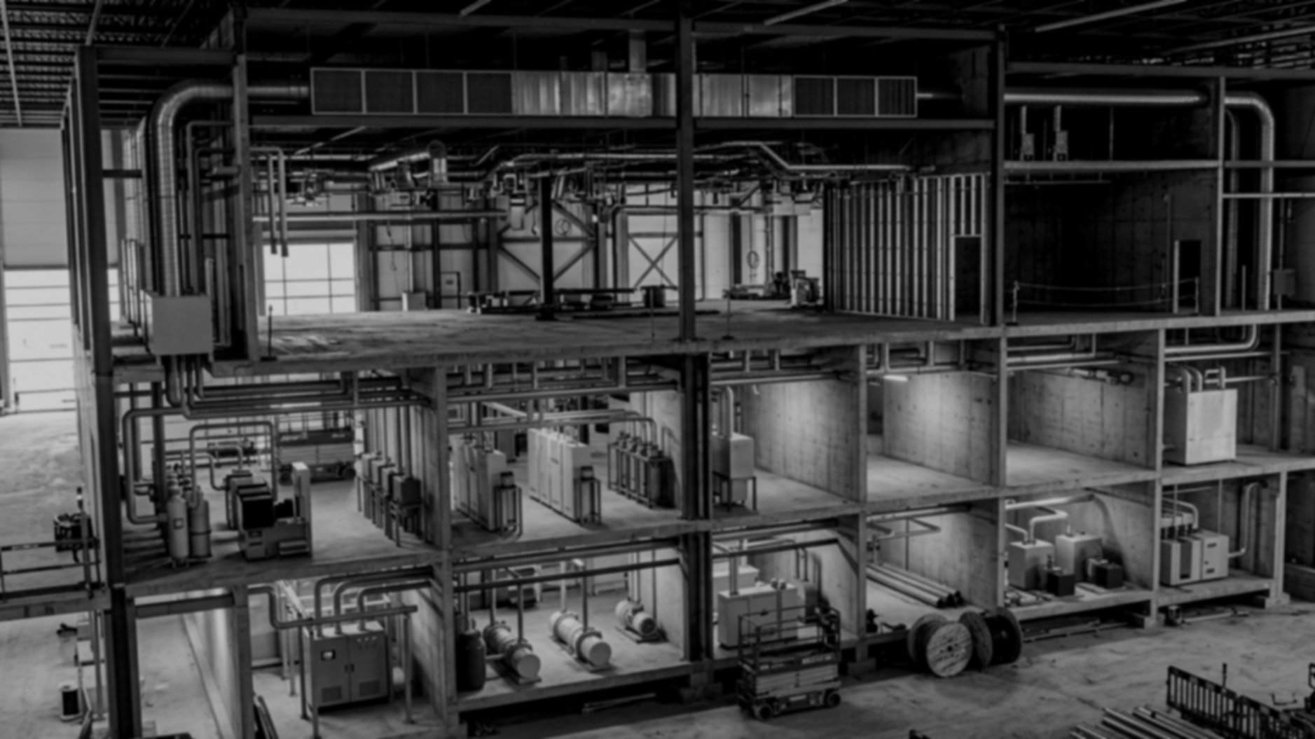
Facility & Cleanroom Development
Greenfield planning through full-scale production. Layout, ISO classification, tool installation, subfab infrastructure, commissioning, and EH&S compliance.
02
Equipment Engineering
Design, development, installation, and lifecycle support for semiconductor manufacturing equipment in research and high-volume production environments.
03
Process Development & Advanced Materials
Thin-film deposition, advanced materials processing, and novel reactor design optimized for both research and production applications.
04
Subfab & Utility Infrastructure
Layout guidance and equipment selection for vacuum, chillers, abatement, bulk gas, DI water, and electrical distribution systems.
05
Foundations & Structural Analysis
Stable, long-term support for critical semiconductor equipment requires careful consideration of soil behavior, structural dynamics, and vibration control. Our approach evaluates the coupled soil–foundation–machine system to ensure reliable performance for vibration-sensitive tools.
Drag to build